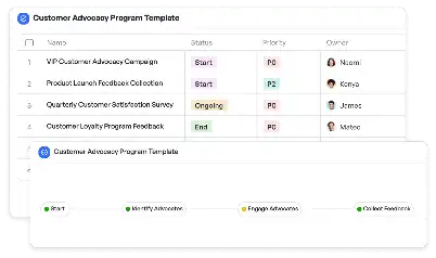
PCB Assembly Defect Analysis Template
Achieve project success with the PCB Assembly Defect Analysis Template today!

What is PCB Assembly Defect Analysis Template?
The PCB Assembly Defect Analysis Template is a specialized tool designed to streamline the identification, analysis, and resolution of defects in printed circuit board (PCB) assemblies. In the electronics manufacturing industry, ensuring the quality and reliability of PCBs is critical, as they form the backbone of most electronic devices. This template provides a structured approach to documenting defects, analyzing root causes, and implementing corrective actions. By leveraging this template, teams can address issues such as soldering defects, component misalignment, and electrical failures, which are common in PCB assembly processes. The template is particularly valuable in high-stakes industries like automotive, aerospace, and medical devices, where PCB reliability is non-negotiable.
Try this template now
Who is this PCB Assembly Defect Analysis Template Template for?
This template is ideal for professionals involved in electronics manufacturing and quality assurance. Typical users include quality engineers, production managers, and R&D teams who need to ensure the integrity of PCB assemblies. It is also beneficial for suppliers and contractors who must meet stringent quality standards set by their clients. Additionally, this template serves as a valuable resource for training new team members, providing them with a clear framework for understanding and addressing PCB assembly defects.

Try this template now
Why use this PCB Assembly Defect Analysis Template?
The PCB Assembly Defect Analysis Template addresses specific pain points in the PCB manufacturing process. For instance, it helps teams systematically identify and categorize defects, reducing the risk of overlooking critical issues. The template also facilitates root cause analysis, enabling teams to pinpoint the underlying reasons for defects, such as material inconsistencies or process errors. Furthermore, it provides a structured format for planning and implementing corrective actions, ensuring that solutions are both effective and sustainable. By using this template, organizations can minimize production downtime, reduce waste, and enhance the overall quality of their PCB assemblies.

Try this template now
Get Started with the PCB Assembly Defect Analysis Template
Follow these simple steps to get started with Meegle templates:
1. Click 'Get this Free Template Now' to sign up for Meegle.
2. After signing up, you will be redirected to the PCB Assembly Defect Analysis Template. Click 'Use this Template' to create a version of this template in your workspace.
3. Customize the workflow and fields of the template to suit your specific needs.
4. Start using the template and experience the full potential of Meegle!
Try this template now
Free forever for teams up to 20!
The world’s #1 visualized project management tool
Powered by the next gen visual workflow engine


