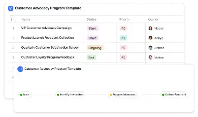
Semiconductor Bump Planarity Control
Achieve project success with the Semiconductor Bump Planarity Control today!

What is Semiconductor Bump Planarity Control?
Semiconductor Bump Planarity Control refers to the process of ensuring uniformity and flatness in the bumps on semiconductor wafers. These bumps are critical for establishing electrical connections between the chip and the substrate in advanced packaging technologies. The importance of bump planarity lies in its direct impact on the reliability and performance of semiconductor devices. Uneven bumps can lead to poor connections, signal integrity issues, and even device failure. In the context of modern semiconductor manufacturing, where miniaturization and high-density packaging are the norms, achieving precise bump planarity is a challenging yet essential task. This template is designed to streamline the process, providing a structured approach to assess, analyze, and optimize bump planarity in various manufacturing scenarios.
Try this template now
Who is this Semiconductor Bump Planarity Control Template for?
This template is ideal for professionals in the semiconductor industry, including process engineers, quality assurance teams, and R&D specialists. It is particularly useful for those involved in advanced packaging, wafer-level manufacturing, and device testing. Typical roles that benefit from this template include semiconductor fabrication engineers, packaging specialists, and quality control analysts. By using this template, these professionals can ensure that their processes meet the stringent requirements of modern semiconductor manufacturing, thereby enhancing product reliability and performance.

Try this template now
Why use this Semiconductor Bump Planarity Control?
The primary advantage of using this template is its ability to address specific challenges in bump planarity control. For instance, uneven bump heights can cause misalignment during chip assembly, leading to defective products. This template provides a systematic approach to identify and rectify such issues, ensuring uniform bump heights across the wafer. Additionally, it helps in optimizing the manufacturing process by identifying key variables that influence bump planarity, such as deposition techniques and material properties. By addressing these pain points, the template not only improves product quality but also reduces the risk of costly rework and delays in production.

Try this template now
Get Started with the Semiconductor Bump Planarity Control
Follow these simple steps to get started with Meegle templates:
1. Click 'Get this Free Template Now' to sign up for Meegle.
2. After signing up, you will be redirected to the Semiconductor Bump Planarity Control. Click 'Use this Template' to create a version of this template in your workspace.
3. Customize the workflow and fields of the template to suit your specific needs.
4. Start using the template and experience the full potential of Meegle!
Try this template now
Free forever for teams up to 20!
The world’s #1 visualized project management tool
Powered by the next gen visual workflow engine


