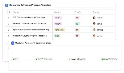
Semiconductor Process Window Analysis
Achieve project success with the Semiconductor Process Window Analysis today!

What is Semiconductor Process Window Analysis?
Semiconductor Process Window Analysis is a critical methodology used in the semiconductor manufacturing industry to identify the optimal operating conditions for various processes such as lithography, etching, and deposition. This analysis ensures that the manufacturing process remains within a defined 'window' where the output meets quality and performance standards. By leveraging advanced statistical tools and simulation techniques, engineers can pinpoint the parameters that yield the highest efficiency and minimal defects. For instance, in lithography, the process window might involve the precise calibration of exposure dose and focus to achieve the desired pattern fidelity. The importance of this analysis cannot be overstated, as it directly impacts yield, cost, and the overall reliability of semiconductor devices.
Try this template now
Who is this Semiconductor Process Window Analysis Template for?
This Semiconductor Process Window Analysis template is designed for professionals in the semiconductor industry, including process engineers, quality assurance teams, and R&D specialists. It is particularly beneficial for those involved in optimizing manufacturing processes, troubleshooting defects, and improving yield. Typical roles that would find this template invaluable include lithography engineers, etch process specialists, and deposition technologists. Additionally, it serves as a vital tool for project managers overseeing semiconductor production lines, enabling them to streamline workflows and ensure consistent quality across batches.

Try this template now
Why use this Semiconductor Process Window Analysis?
The Semiconductor Process Window Analysis template addresses several pain points unique to the semiconductor manufacturing process. For example, maintaining process stability in high-volume production environments can be challenging due to variations in equipment performance and material properties. This template provides a structured approach to identify and mitigate these variations, ensuring consistent output. It also helps in reducing the time and cost associated with trial-and-error methods by offering a data-driven framework for process optimization. Furthermore, the template facilitates cross-functional collaboration by providing a common language and set of tools for engineers, technicians, and managers. By using this template, organizations can achieve higher yields, lower defect rates, and faster time-to-market for their semiconductor products.

Try this template now
Get Started with the Semiconductor Process Window Analysis
Follow these simple steps to get started with Meegle templates:
1. Click 'Get this Free Template Now' to sign up for Meegle.
2. After signing up, you will be redirected to the Semiconductor Process Window Analysis. Click 'Use this Template' to create a version of this template in your workspace.
3. Customize the workflow and fields of the template to suit your specific needs.
4. Start using the template and experience the full potential of Meegle!
Try this template now
Free forever for teams up to 20!
The world’s #1 visualized project management tool
Powered by the next gen visual workflow engine


