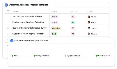
Wafer-Level Burn-In Optimization
Achieve project success with the Wafer-Level Burn-In Optimization today!

What is Wafer-Level Burn-In Optimization?
Wafer-Level Burn-In Optimization refers to the process of applying stress tests to semiconductor wafers at the wafer level to identify and eliminate potential defects before packaging. This process is critical in the semiconductor industry as it ensures the reliability and longevity of integrated circuits. By conducting burn-in tests at the wafer level, manufacturers can detect early failures, reduce costs associated with defective packaging, and improve overall product quality. The optimization aspect involves fine-tuning the parameters of the burn-in process, such as temperature, voltage, and duration, to achieve maximum efficiency and effectiveness. This is particularly important in high-demand industries like automotive and aerospace, where component reliability is paramount.
Try this template now
Who is this Wafer-Level Burn-In Optimization Template for?
This template is designed for professionals in the semiconductor industry, including process engineers, quality assurance teams, and R&D specialists. It is particularly useful for teams working on advanced semiconductor manufacturing processes, where precision and reliability are critical. Typical roles that would benefit from this template include wafer fabrication engineers, reliability engineers, and product managers overseeing the development of high-performance integrated circuits. By using this template, these professionals can streamline their workflows, ensure compliance with industry standards, and achieve better outcomes in wafer-level burn-in processes.

Try this template now
Why use this Wafer-Level Burn-In Optimization?
The Wafer-Level Burn-In Optimization template addresses several key challenges in the semiconductor manufacturing process. One major pain point is the high cost and time associated with identifying defects after packaging. By optimizing the burn-in process at the wafer level, this template helps manufacturers detect and address issues early, saving both time and resources. Another challenge is ensuring the reliability of components in high-stress environments. This template provides a structured approach to fine-tuning burn-in parameters, ensuring that components meet stringent reliability standards. Additionally, the template facilitates better collaboration among cross-functional teams, enabling them to share insights and make data-driven decisions. Overall, it is an indispensable tool for achieving excellence in wafer-level burn-in processes.

Try this template now
Get Started with the Wafer-Level Burn-In Optimization
Follow these simple steps to get started with Meegle templates:
1. Click 'Get this Free Template Now' to sign up for Meegle.
2. After signing up, you will be redirected to the Wafer-Level Burn-In Optimization. Click 'Use this Template' to create a version of this template in your workspace.
3. Customize the workflow and fields of the template to suit your specific needs.
4. Start using the template and experience the full potential of Meegle!
Try this template now
Free forever for teams up to 20!
The world’s #1 visualized project management tool
Powered by the next gen visual workflow engine


