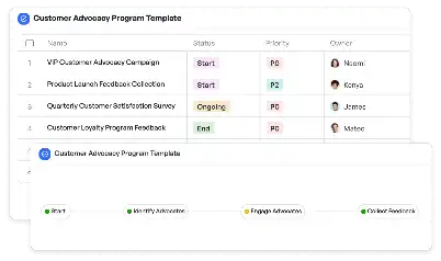
Semiconductor Process Variability Map
Achieve project success with the Semiconductor Process Variability Map today!

What is Semiconductor Process Variability Map?
The Semiconductor Process Variability Map is a critical tool in the semiconductor industry, designed to identify, analyze, and mitigate variability in manufacturing processes. Variability in semiconductor processes can arise from numerous factors, including material inconsistencies, equipment performance, and environmental conditions. This map provides a structured approach to visualize and address these variabilities, ensuring higher yield and performance reliability. For instance, in advanced nodes like 5nm or 3nm, even minor variations can lead to significant performance degradation or yield loss. By leveraging this map, engineers can pinpoint the root causes of variability and implement corrective actions effectively.
Try this template now
Who is this Semiconductor Process Variability Map Template for?
This template is tailored for professionals in the semiconductor industry, including process engineers, quality assurance teams, and R&D specialists. It is particularly beneficial for those working on advanced process nodes, where variability management is crucial. Typical roles include fabrication engineers analyzing wafer-level data, design engineers ensuring process compatibility, and quality teams monitoring defect densities. Whether you are optimizing a new process node or troubleshooting an existing one, this template provides the necessary framework to address variability challenges.

Try this template now
Why use this Semiconductor Process Variability Map?
Variability in semiconductor processes can lead to significant challenges, such as reduced yield, increased defect rates, and performance inconsistencies. The Semiconductor Process Variability Map addresses these pain points by offering a comprehensive framework to identify and mitigate variability sources. For example, it helps in correlating defect densities with process parameters, enabling targeted improvements. Additionally, it supports simulation-based approaches to predict variability impacts, allowing proactive adjustments. By using this template, teams can ensure process robustness, enhance product reliability, and maintain competitive advantage in the rapidly evolving semiconductor industry.

Try this template now
Get Started with the Semiconductor Process Variability Map
Follow these simple steps to get started with Meegle templates:
1. Click 'Get this Free Template Now' to sign up for Meegle.
2. After signing up, you will be redirected to the Semiconductor Process Variability Map. Click 'Use this Template' to create a version of this template in your workspace.
3. Customize the workflow and fields of the template to suit your specific needs.
4. Start using the template and experience the full potential of Meegle!
Try this template now
Free forever for teams up to 20!
The world’s #1 visualized project management tool
Powered by the next gen visual workflow engine


