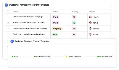
Wafer Fab Process Integration
Achieve project success with the Wafer Fab Process Integration today!

What is Wafer Fab Process Integration?
Wafer Fab Process Integration refers to the meticulous coordination of various fabrication steps in semiconductor manufacturing to ensure the production of high-quality wafers. This process is critical in the semiconductor industry as it involves integrating multiple complex steps such as lithography, etching, deposition, and doping. Each step must be precisely aligned to achieve the desired electrical properties and functionality of the semiconductor devices. The importance of Wafer Fab Process Integration lies in its ability to minimize defects, optimize yield, and ensure the reliability of the final product. For instance, in the production of advanced nodes like 5nm or 3nm technology, the integration process becomes even more challenging due to the reduced feature sizes and increased complexity. This template provides a structured approach to manage these challenges effectively.
Try this template now
Who is this Wafer Fab Process Integration Template for?
This Wafer Fab Process Integration Template is designed for professionals in the semiconductor industry, including process engineers, integration specialists, and quality assurance teams. It is particularly useful for those involved in the development and production of advanced semiconductor devices. Typical roles that benefit from this template include lithography engineers who need to align patterns accurately, etching specialists who ensure precise material removal, and deposition experts who manage thin film applications. Additionally, it is valuable for project managers overseeing the entire wafer fabrication process, ensuring that all steps are seamlessly integrated to meet production goals.

Try this template now
Why use this Wafer Fab Process Integration?
The Wafer Fab Process Integration template addresses several critical pain points in semiconductor manufacturing. One major challenge is managing the interdependencies between different fabrication steps, which can lead to defects if not properly coordinated. This template provides a clear framework to map out these dependencies, reducing the risk of errors. Another issue is the need for real-time monitoring and adjustment of process parameters to maintain consistency. The template includes tools for tracking and analyzing data, enabling timely interventions. Furthermore, as semiconductor devices become more complex, the integration process requires collaboration across multiple teams and disciplines. This template facilitates communication and collaboration, ensuring that all stakeholders are aligned. By using this template, organizations can achieve higher yields, better product reliability, and faster time-to-market for their semiconductor devices.

Try this template now
Get Started with the Wafer Fab Process Integration
Follow these simple steps to get started with Meegle templates:
1. Click 'Get this Free Template Now' to sign up for Meegle.
2. After signing up, you will be redirected to the Wafer Fab Process Integration. Click 'Use this Template' to create a version of this template in your workspace.
3. Customize the workflow and fields of the template to suit your specific needs.
4. Start using the template and experience the full potential of Meegle!
Try this template now
Free forever for teams up to 20!
The world’s #1 visualized project management tool
Powered by the next gen visual workflow engine


