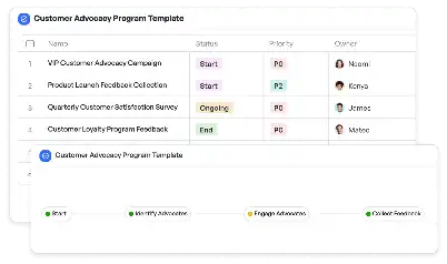
Semiconductor Lithography Process Flow
Achieve project success with the Semiconductor Lithography Process Flow today!

What is Semiconductor Lithography Process Flow?
Semiconductor Lithography Process Flow refers to the intricate sequence of steps involved in transferring circuit patterns onto a semiconductor wafer. This process is pivotal in the manufacturing of microchips, which power everything from smartphones to supercomputers. The flow typically includes stages such as mask preparation, photoresist application, exposure, development, etching, and final inspection. Each step requires precision and adherence to strict quality standards to ensure the production of high-performance and reliable chips. The importance of this process lies in its ability to define the critical dimensions and features of the semiconductor devices, making it a cornerstone of the electronics industry.
Try this template now
Who is this Semiconductor Lithography Process Flow Template for?
This template is designed for professionals and teams involved in semiconductor manufacturing and research. Typical users include process engineers, photolithography specialists, quality assurance teams, and R&D personnel. It is also valuable for project managers overseeing semiconductor fabrication projects. By providing a structured workflow, this template helps these roles coordinate effectively, ensuring that each stage of the lithography process is executed flawlessly.

Try this template now
Why use this Semiconductor Lithography Process Flow?
The Semiconductor Lithography Process Flow template addresses several pain points in the industry. For instance, the complexity of aligning masks and applying photoresist can lead to errors if not managed properly. This template provides a clear roadmap for each step, reducing the likelihood of mistakes. Additionally, it helps streamline communication between teams, ensuring that everyone is aligned on the process requirements. By using this template, organizations can achieve higher yields, better quality control, and faster time-to-market for their semiconductor products.

Try this template now
Get Started with the Semiconductor Lithography Process Flow
Follow these simple steps to get started with Meegle templates:
1. Click 'Get this Free Template Now' to sign up for Meegle.
2. After signing up, you will be redirected to the Semiconductor Lithography Process Flow. Click 'Use this Template' to create a version of this template in your workspace.
3. Customize the workflow and fields of the template to suit your specific needs.
4. Start using the template and experience the full potential of Meegle!
Try this template now
Free forever for teams up to 20!
The world’s #1 visualized project management tool
Powered by the next gen visual workflow engine


