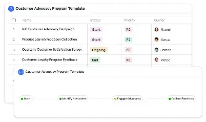
Semiconductor Process Flow Control
Achieve project success with the Semiconductor Process Flow Control today!

What is Semiconductor Process Flow Control?
Semiconductor Process Flow Control refers to the systematic management and optimization of processes involved in semiconductor manufacturing. This includes wafer fabrication, photolithography, etching, deposition, and other critical steps. Given the complexity and precision required in semiconductor production, effective process flow control ensures minimal defects, higher yields, and consistent quality. For instance, in photolithography, precise control over exposure and alignment is crucial to achieve the desired circuit patterns. Without robust process flow control, manufacturers risk increased defects, reduced efficiency, and higher costs. This template is designed to address these challenges by providing a structured approach to managing each step in the semiconductor manufacturing process.
Try this template now
Who is this Semiconductor Process Flow Control Template for?
This template is ideal for professionals involved in semiconductor manufacturing, including process engineers, quality assurance teams, and production managers. It is particularly useful for those working in wafer fabrication facilities, photolithography labs, and quality control departments. For example, a process engineer can use this template to design and monitor workflows for etching and deposition, while a quality assurance team can leverage it to ensure compliance with industry standards. Additionally, production managers can utilize the template to streamline operations and improve communication across teams.

Try this template now
Why use this Semiconductor Process Flow Control?
Semiconductor manufacturing presents unique challenges, such as maintaining precision in photolithography, ensuring uniformity in deposition, and minimizing defects during etching. This template addresses these pain points by offering a comprehensive framework for process flow control. For instance, it includes tools for real-time monitoring of critical parameters, such as temperature and pressure, which are essential for maintaining process stability. It also provides guidelines for defect analysis and mitigation, helping manufacturers identify and address issues before they escalate. By using this template, teams can achieve higher yields, reduce waste, and maintain the high standards required in semiconductor production.

Try this template now
Get Started with the Semiconductor Process Flow Control
Follow these simple steps to get started with Meegle templates:
1. Click 'Get this Free Template Now' to sign up for Meegle.
2. After signing up, you will be redirected to the Semiconductor Process Flow Control. Click 'Use this Template' to create a version of this template in your workspace.
3. Customize the workflow and fields of the template to suit your specific needs.
4. Start using the template and experience the full potential of Meegle!
Try this template now
Free forever for teams up to 20!
The world’s #1 visualized project management tool
Powered by the next gen visual workflow engine


