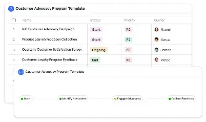
Semiconductor EDA Toolchain Configuration
Achieve project success with the Semiconductor EDA Toolchain Configuration today!

What is Semiconductor EDA Toolchain Configuration?
Semiconductor EDA Toolchain Configuration refers to the structured setup and integration of Electronic Design Automation (EDA) tools tailored for semiconductor design and manufacturing. This configuration is critical in managing the complex workflows involved in designing integrated circuits (ICs), from schematic capture to physical layout and verification. The importance of this configuration lies in its ability to streamline processes, reduce errors, and ensure compatibility across various tools. For instance, in the design of a 5nm node chip, the toolchain must handle intricate design rules, power optimization, and timing analysis. By leveraging a well-configured EDA toolchain, engineers can efficiently navigate these challenges, ensuring high-quality designs and faster time-to-market.
Try this template now
Who is this Semiconductor EDA Toolchain Configuration Template for?
This template is designed for semiconductor design engineers, project managers, and EDA tool specialists. It is particularly beneficial for teams working on advanced node designs, such as 5nm or 3nm, where precision and tool compatibility are paramount. Typical roles include IC design engineers, verification engineers, and CAD tool administrators. For example, a team developing an AI accelerator chip can use this template to coordinate tasks across design, simulation, and verification stages, ensuring seamless collaboration and efficient resource utilization.

Try this template now
Why use this Semiconductor EDA Toolchain Configuration?
The Semiconductor EDA Toolchain Configuration template addresses specific pain points in the semiconductor design process. For instance, managing tool compatibility across different vendors can be challenging, leading to integration issues and delays. This template provides a standardized approach to toolchain setup, ensuring all tools work harmoniously. Additionally, it helps in automating repetitive tasks, such as design rule checks and layout versus schematic verification, saving valuable engineering time. Another advantage is its ability to handle the increasing complexity of modern IC designs, such as multi-die systems and advanced packaging. By using this template, teams can focus on innovation rather than troubleshooting toolchain issues, ultimately delivering better products faster.

Try this template now
Get Started with the Semiconductor EDA Toolchain Configuration
Follow these simple steps to get started with Meegle templates:
1. Click 'Get this Free Template Now' to sign up for Meegle.
2. After signing up, you will be redirected to the Semiconductor EDA Toolchain Configuration. Click 'Use this Template' to create a version of this template in your workspace.
3. Customize the workflow and fields of the template to suit your specific needs.
4. Start using the template and experience the full potential of Meegle!
Try this template now
Free forever for teams up to 20!
The world’s #1 visualized project management tool
Powered by the next gen visual workflow engine


