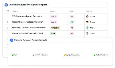
Semiconductor DFT Coverage Analyzer
Achieve project success with the Semiconductor DFT Coverage Analyzer today!

What is Semiconductor DFT Coverage Analyzer?
The Semiconductor DFT (Design for Testability) Coverage Analyzer is a specialized tool designed to evaluate and optimize the test coverage of semiconductor designs. In the semiconductor industry, ensuring high fault coverage is critical to delivering reliable and defect-free chips. This tool provides a comprehensive analysis of test patterns and fault simulations, enabling engineers to identify gaps in coverage and improve the overall quality of the design. By leveraging advanced algorithms and industry-specific methodologies, the Semiconductor DFT Coverage Analyzer plays a pivotal role in reducing time-to-market and ensuring compliance with stringent quality standards. For example, in the development of AI processors, this tool helps ensure that every logic gate and interconnect is thoroughly tested, minimizing the risk of undetected faults in production.
Try this template now
Who is this Semiconductor DFT Coverage Analyzer Template for?
The Semiconductor DFT Coverage Analyzer template is tailored for professionals in the semiconductor industry, including design engineers, test engineers, and quality assurance teams. It is particularly beneficial for those working on complex chip designs, such as AI processors, automotive chips, and IoT devices, where high fault coverage is paramount. Typical roles that benefit from this template include DFT engineers responsible for creating and validating test patterns, test managers overseeing the fault simulation process, and quality assurance specialists ensuring compliance with industry standards. Whether you are working on a cutting-edge 5G modem or a high-performance GPU, this template provides the structure and tools needed to streamline your DFT coverage analysis process.

Try this template now
Why use this Semiconductor DFT Coverage Analyzer?
The Semiconductor DFT Coverage Analyzer addresses several critical pain points in the semiconductor design process. One of the primary challenges is identifying and addressing gaps in test coverage, which can lead to undetected faults and costly rework. This template provides a systematic approach to analyzing test patterns and fault simulations, ensuring comprehensive coverage. Another common issue is the complexity of managing multiple test scenarios and data sets. The template simplifies this process by organizing tasks into clear, actionable steps, from requirement analysis to report generation. Additionally, it helps teams stay aligned and focused on quality objectives, reducing the risk of errors and ensuring that the final product meets or exceeds industry standards. By using this template, semiconductor professionals can confidently tackle the challenges of DFT coverage analysis and deliver high-quality, reliable chips.

Try this template now
Get Started with the Semiconductor DFT Coverage Analyzer
Follow these simple steps to get started with Meegle templates:
1. Click 'Get this Free Template Now' to sign up for Meegle.
2. After signing up, you will be redirected to the Semiconductor DFT Coverage Analyzer. Click 'Use this Template' to create a version of this template in your workspace.
3. Customize the workflow and fields of the template to suit your specific needs.
4. Start using the template and experience the full potential of Meegle!
Try this template now
Free forever for teams up to 20!
The world’s #1 visualized project management tool
Powered by the next gen visual workflow engine


